


OrCAD是最好,最專業的軟體模擬,電子電路分析和電子設計自動化軟體套件之一,可以滿足不同行業的使用者進行模擬和高端電路設計操作的需要。
它於1999年被Cadence Design Systems收購,並從2005年開始與Cadence Allegro整合。
從那時起,Cadence(又名Allegro,OrCAD,PSPICE,Cadence OrCAD,Cadence Allegro)逐漸成為一個大型EDA軟體套件,其中包括足以涵蓋EDA設計各個方面的工具。
它可以滿足幾乎所有的電子設計要求,內含ASIC設計,FPGA設計和PCB板設計。它在電路模擬,電路圖設計,自動佈局和佈線,佈局設計和驗證等方面具有絕對優勢。
Cadence內含原理圖編輯器(捕獲),模擬/混合信號電路模擬器(PSpice)和PCB板佈局解決專案(PCB Designer Professional)。
電子設計專案師和電子技術人員主要使用它來建立電子原理圖,執行混合信號模擬以及用於製造印刷電路板的電子印刷品。
Cadence能夠進行高速電路板設計和模擬測試,改善PCB設計流程,並且在板圖繪製功能方面大大超過了許多類似軟體。
它具有交談式工作介面和全面的功能,為高速,高密度,多層複雜的PCB設計和佈線提供了最完美的解決專案。
此外,Cadence提供的強大的輸入/輸出功能使與其他關聯軟體(如ADIVA,UGS(Fabmaster),VALOR,Agilent ADS,DXF,IDF等)的通信非常方便。
【電子電路分析和電子設計】Cadence 17.40主要特徵:
合適的圖形使用者環境和使用圖示的顯示電路
在強大的環境中OrCAD Capture和Capture CIS原理圖設計電路
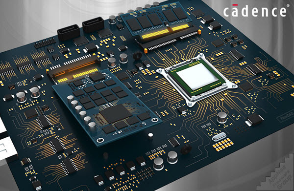
設計PCB的能力(印刷電路板架,是指電路板或PCB)
擁有豐富的零組件和電子裝置庫
圖形環境PSpice中的進階模擬和分析電子電路
環境Orcad PCB設計器/編輯器,用於設計和編輯PCB
與MATLAB和Simulink軟體進行互動的能力

【電子電路分析和電子設計】Cadence 17.40 官網下載:
https://www.cadence.com/zh_TW/home.html
OrCAD is one of the best and most professional software simulation, electronic circuits analysis, and electronic design automation software suite, which can satisfy users of different industries for simulation and high-end circuit design operation. It was acquired by Cadence Design Systems in 1999, and has been integrated with Cadence Allegro since 2005.
From then on, Cadence (AKA: Allegro, OrCAD, PSPICE, Cadence OrCAD, Cadence Allegro) gradually became a large EDA software suite, which contains enough tools to cover all aspects of EDA design. It can accomplish almost all kinds of electronic design requirements, including ASIC design, FPGA design and PCB board design. It has absolute advantages in circuit simulation, circuit diagram design, automatic layout & routing, layout design and verification, etc.
Cadence includes a schematic editor (Capture), an analog/mixed-signal circuit simulator (PSpice) and a PCB board layout solution (PCB Designer Professional). It is mainly used by electronic design engineers and electronic technicians to create electronic schematics, perform mixed-signal simulation and electronic prints for manufacturing printed circuit boards.
Cadence is able to carry out high-speed circuit board design and simulation test, optimize PCB design process, and it exceeds many similar software by a large amount in terms of board drawing functions. It comes with interactive working interface and comprehensive features, providing the most perfect solution for high-speed, high-density, multi-layer complex PCB design and routing. In addition, the powerful input/output function provided by Cadence makes it very convenient to communicate with other related software, such as ADIVA, UGS (Fabmaster), VALOR, Agilent ADS, DXF, IDF, etc.
// Key Features //
Suitable graphical user environments and display circuit using icons
OrCAD Capture and Capture CIS schematic design circuits in powerful environment
Ability to design PCB (Printed Circuit Board stands and means the board or PCB)
Has an extensive library full of components and electronic devices
Advanced simulation and analysis electronic circuits in a graphical environment PSpice
Environment Orcad PCB Designer / Editor to design and edit PCB
Ability to interact with MATLAB and Simulink software