

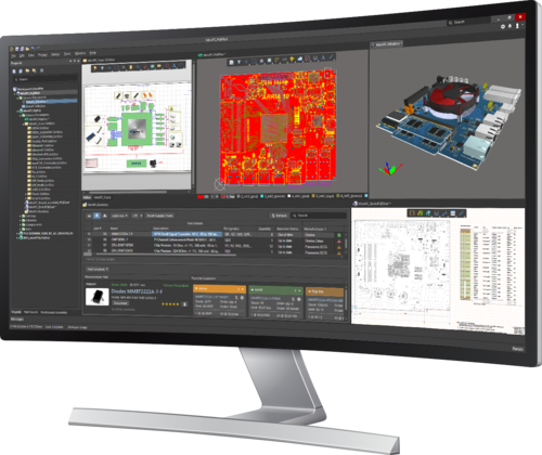
Altium NEXUS 它是用於電子印刷電路板設計的完整,端到端設計環境。
Altium NEXUS 使您可以在最有效和協作的PCB設計環境中實現您的想法。
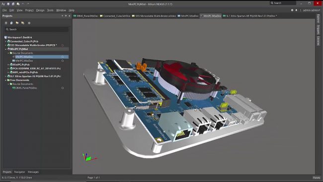
從用於助聽器的可折疊的小巧柔韌性板到20層以上的大型高速網絡路由器,Altium NEXUS均可與您一起提供成功的設計。
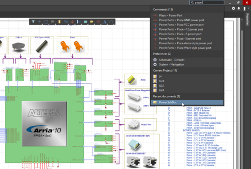
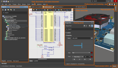
在Altium NEXUS中的工作方式與其他Windows應用程序非常相似,可以通過熟悉的菜單訪問命令,可以使用標準的Windows鍵盤和鼠標操作來縮放和平移圖形視圖,並且可以通過鍵盤快捷鍵訪問許多命令和功能。
【電子印刷電路板設計】Altium Nexus 3的功能:
以下是安裝Altium Nexus 3後可以體驗的一些令人驚奇的功能,請記住這些功能可能會有所不同,並且完全取決於您的系統是否支持它們。
現在,可以使用新的“引腳”面板在“單組件編輯器”中使用“組件引腳到多個焊盤的映射”。
現在可以給備用原理圖元件符號一個用戶定義的名稱。
PCB組件間隙設計規則的其他選項–現在,您可以排除不具有3D實體的組件,也可以選擇使用組件邊界檢查間隙。
現在,內部平面可以使用與放置在信號層上的多邊形相同的澆注算法,從而改善形狀定義和焊盤/通孔連接。
嵌入式板陣列現在支持以任意角度放置陣列。
新的PCB專用線串,用於層厚。
快速路由和快速差分對路由工具可提供響應速度更快的交互式路由。
更新了ODBᐩᐩ設置對話框-更好地控制機械層數據如何合併到輸出中。
新的矩形對像已添加到PCB編輯器的“位置”菜單中。
通過新的“放置»圖形”命令,可以更簡單地在PCB上放置圖形。
數字鍵盤支持3D視圖移動和旋轉動作。
機械層現在可以包含在3D中–是註釋3D圖像的理想選擇。
新的“導出”命令可將3D PCB輸出為圖像-用戶可以控制格式和圖像分辨率。
【電子印刷電路板設計】Altium Nexus 3 官網下載:
https://www.altium.com/documentation/altium-nexus/new-in-altium-nexus
Welcome to Altium NEXUS, which is a complete, end-to-end design environment for electronic printed circuit board design.
Altium NEXUS enables you to bring your ideas to life with the most efficient and collaborative PCB design environment available.
From a tiny, foldable rigid-flex board that goes into a hearing aid, to a large, 20+ layer high-speed network router, Altium NEXUS works with you to deliver a successful design.
The way you work in Altium NEXUS is much like other Windows applications in that commands are accessed through familiar menus,
graphical views can be zoomed and panned using standard Windows keyboard and mouse actions, and many of the commands and features can be accessed through keyboard shortcuts.
Features of Altium Nexus 3
Below are some amazing features you can experience after installation of Altium Nexus 3 please keep in mind features may vary and totally depends if your system supports them.
Component Pin to Multiple Pad Mapping is now available in the Single Component Editor, using the new Pins panel.
Alternate schematic component symbols can now be given a user-defined name.
Additional options for the PCB Component Clearance design rule – you can now exclude components without a 3D Body from being checked, as well as choose to have clearance checked using the component boundary.
Internal planes can now use the same pouring algorithm as polygons placed on a signal layer, giving improved shape definition and pad/via connections.
Embedded Board Arrays now support array placement at any angle.
New PCB Special String For Layer Thickness.
Quick Routing and Quick Differential Pair Routing Tools for more responsive interactive routing.
Updated ODBᐩᐩ Setup Dialog – giving better control of how mechanical layer data is merged into the outputs.
A new rectangle object has been added to the PCB Editor’s Place menu.
Simpler process of placing a Graphic on the PCB, via the new Place » Graphic command.
Numerical keypad support for 3D View Move and Rotate actions.
Mechanical Layers can now be included in the 3D – ideal for annotating the 3D image.
New Export command to output the 3D PCB as an image – with user control over the format and image resolution.